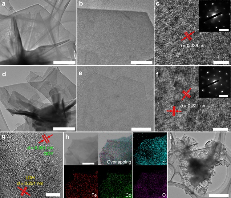
Fig. 3.
TEM characterization of electrocatalyst samples. a Low-magnification, b high-magnification, and c high-resolution TEM images and corresponding selected-area electron diffraction pattern (SAED, inset to c of pure ICLDH nanosheets. Scale bars: a 1 μm; b 300 nm; c 5 nm; inset of c, 5 1/nm. d Low-magnification, e high-magnification, and f, g high-resolution TEM images of e-ICLDH@GDY nanosheets (inset to f SAED pattern of e-ICLDH@GDY). Scale bars: d 200 nm; e 100 nm; f and g 5 nm; inset of f 5 1/nm. h Typical scanning TEM and corresponding elemental mapping images of C, Fe, Co, and O atoms in the e-ICLDH@GDY nanosheets. Scale bars: h 100 nm. i TEM image of the GDY coatings after removal of the ICLDH from the sample. Scale bars: i 500 nm

