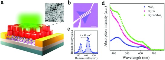
Figure 1.

Schematic model of the device and optical characterization of the PQDs/MoS2 MvdWH. a) Schematic model of the device with its inset shows a typical TEM image of the PQDs. The scale bar is 50 nm. b) Optical image of the as‐fabricated device. The scale bar is 10 µm. c) Raman spectra of pristine MoS2 monolayer. d) UV–vis absorption of the pristine MoS2, pure PQDs, and the MvdWH.
