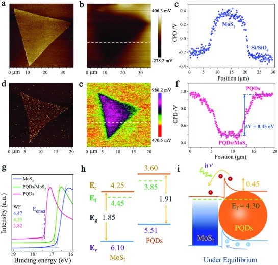
Figure 2.

KPFM characterization and UPS experimentally determined energy level diagram of the PQDs/MoS2 MvdWH. a,d) Topography profile, b,e) spatial maps of the contact potential difference (CPD), and c,f) line profiles of CPD along the white dotted line marked in panels (b) and (e) for pristine MoS2 and PQDs/MoS2 MvdWH, respectively. g) The WF measured by UPS. h) Energy level diagrams for PQDs and MoS2 before contact and i) band diagram for PQDs/MoS2 heterojunction under equilibrium in dark.
