Figure 3.

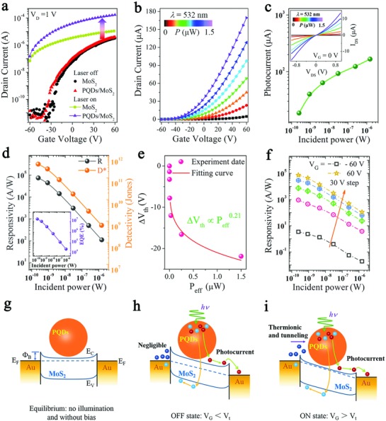
Optoelectronic performance and the schematic of channel current transport mechanism. a) Transfer characteristics for pristine MoS2 and PQDs/MoS2 hybrid phototransistors both in dark and under illumination of 532 nm at V D = 1 V. b) Photoinduced transfer characteristics of the MvdWH based phototransistor under a range of efficient illumination powers (from dark to 1.5 µW). c) Photocurrent obtained from panel (b) at V G = 60 V. The inset shows the I D–V D curves as a function of illumination powers. d) Photoresponsivity and specific detectivity with an inset shows the EQE as a function of illumination powers of the MvdWH based phototransistor. e) The shift of the threshold voltage (ΔV th) from panel (b) as a function of illumination powers. f) Photoresponsivity as a function of effective illumination powers under a range of gate voltage from −60 to 60 V with a fixed step of 30 V. The schematic of channel current transport mechanism and energy band diagram of the MvdWH based phototransistor under g) equilibrium conditions, h) OFF‐state, and i) ON‐state. E F, E c, E V, and ΦB are the Fermi level energy, minimum conduction band energy, maximum valence band energy, and Schottky barrier height, respectively.
