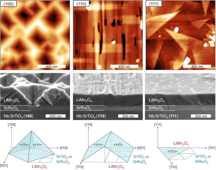
Figure 2.
AFM (top) and SEM (middle) analysis of the surface morphology of 110 nm LiMn2O4 thin films on SrRuO3-coated Nb-SrTiO3 substrates with crystal orientations (100), (110) and (111). SEM images are taken after extensive electrochemical cycling and subsequent cleaning of the surfaces. Schematics (bottom) are shown of the expected crystal facets for the different surface morphologies.

