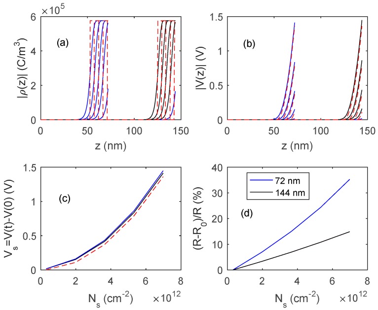
Figure 16.
Distribution of the charge density, ρ (plot (a)) and of the voltage (plot (b)) inside the film as a function of z for different values of charged surface species density, Ns, for two films thickness, 72 nm and 144 nm. Ns in the range (0.3 × 1012 cm−2–7.2 × 1012 cm−2). (c) Surface voltage barrier as a function of the density of charged surface species. Solid lines: proposed model, dashed lines: fully depleted model. (d) Sensor responses to variation of surface charge density. Data for In2O3 are taken from [28,29] Nd = 3.6 × 1018 cm−3.

