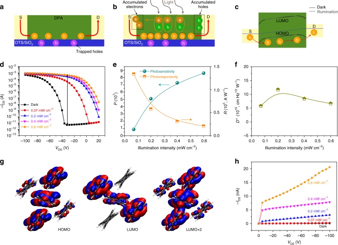
Fig. 3.
Charge transfer mechanism and performance of the phototransistor. Charge transfer mechanism in dark (a) and under illumination (b). c Energy band diagram of electrode/semiconductor interface in dark and under illumination. d Transfer characteristics of DPA-based phototransistor measured under different illumination intensities in the air. e P and R as a function of illumination intensity. f D* as a function of illumination intensity. g Calculated molecular orbitals describing the first electronic excitation (Evert = 388.67 nm; f = 0.1331) at the TD-DFT level. h −IDS at various illumination intensities (VGS = 0 V)

