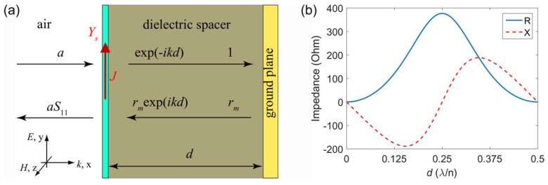
Figure 2.
(a) Schematic illustration of the absorption structure which comprises a ultra-thin sheet, dielectric spacer and metallic ground plane. The amplitude of E field of forward going wave at the ground plane is chosen to be 1 while the amplitude of incident E field is denoted as a. (b) The resistance (R) and reactance (X) of the impedance for PIMS as a function of the dielectric spacer thickness. Reproduced from reference [79], with permission from Optical Society of America, 2011.

