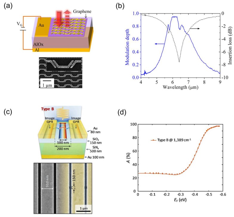
Figure 9.
(a) Top: schematic of the ultrathin optical modulator based on a tunable metasurface absorber. Bottom: a SEM image of the metasurface on graphene. Inset: a zoomed-in view of a portion of the metasurface. (b) The modulation depth achieved experimentally at different wavelength and corresponding insertion loss for the structure shown in (a) [72]. (c) Top: schematic of a perfect absorption structure incorporating graphene plasmonic ribbons and plasmonic metallic antennas. Bottom: a SEM image of the top structure. (d) Absorption of the structure shown in (c) as a function of graphene Fermi level (EF) at the frequency for maximum absorption [73]. Reproduced from references [72,73], with permission from American Chemical Society, 2014; with permission from American Chemical Society, 2018.

