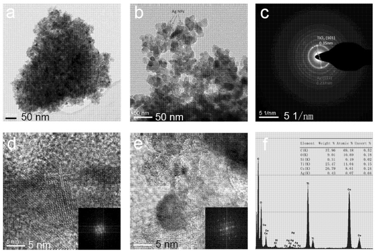
Figure 2.
Transmission electron microscopy with EDS capabilities (TEM) image of the pure TiO2 NPs (a) and Ag@TiO2 NPs-0.5 (b); selected area electron diffraction (SAED) image of Ag@TiO2 NPs-0.5 (c); high-resolution electron microscopy (HRTEM) image taken from TiO2 NPs (d) and the corresponding fast Fourier transform (FFT) mode; HRTEM image taken from Ag NPs (e) and the corresponding FFT mode; EDS of Ag@TiO2 NPs-0.5 (f).

