
Figure 3.
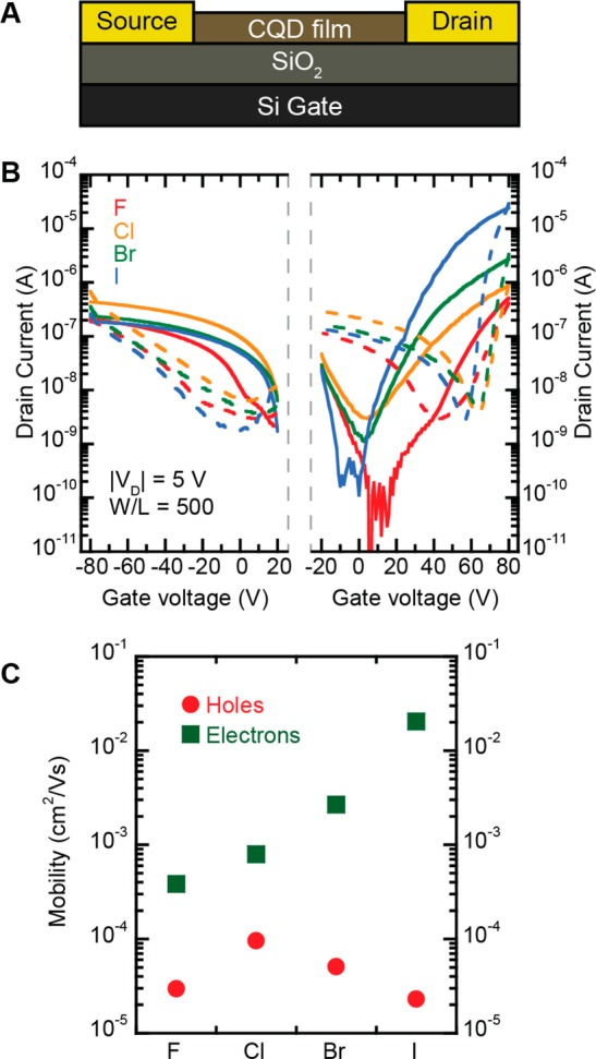
(A) Schematic structure of a PbS CQD FET; (B) transfer characteristics for the p- and n-channel operation of PbS CQD FETs prepared with different halide ligands with the solid lines representing the forward scan and the dashed lines the reverse scans (the color indicates the sample as described in the left panel); (C) comparison of the linear mobility values extracted from the transfer curves.