Fig. 2.
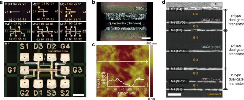
Images of a stacked 3-T device. a Sequential images of the process of printing seven metal layers (scale bar is 1 mm). b A polarized microscopy image of the transistor area (scale bar is 200 μm). c A topographic AFM image (scan area is 100 × 100 μm) measured on top of the channel area. The inset graph shows the profile along the cross-section line. d Cross-sectional SEM image of the stacked 3-T device (M1-7: metal layers, GI1-6: dielectric insulator layers, OSC1-3: organic semiconductor layers, scale bar is 250 nm, Pt was sputtered on the top prior to the SEM measurement)

