
Fig. 4.
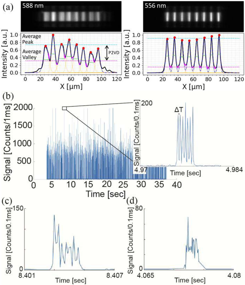
Experimental data collected from MMI waveguide with and without optimized geometries. (a) On the left is an MMI waveguide spot pattern taken from un-optimized waveguide, on the right is the pattern for optimized waveguide which shows uniformly distributed spots. Corresponding plots with analysis confirms improvement in both FWHM and P2VD of the spots after optimization. (b) Fluorescence trace acquired from fluorescently labeled 0.2 μm beads flowing through an optofluidic channel excited at 633 nm. The zoomed in trace shows the pattern of the peaks created by an optimized high-fidelity spot pattern. (c-d) The zoomed in bead traces acquired from un-optimized waveguides where (c) is from a 4.8 μm wide excitation waveguide etched 3 μm deep and (d) is from a 5.5 μm wide excitation waveguide etched 4.2 μm deep.