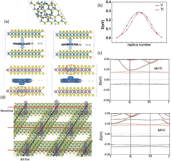
Figure 3.

a) Geometric structure of MP intercalated bilayer MoS2, where the spin distribution is plotted in blue. b) FE switching pathway of TiP/VP intercalated bilayer MoS2. c) Band structure of TiP/VP intercalated bilayer MoS2. d) A design of high‐density RAMs using cross‐point‐array (CPA) structure.
