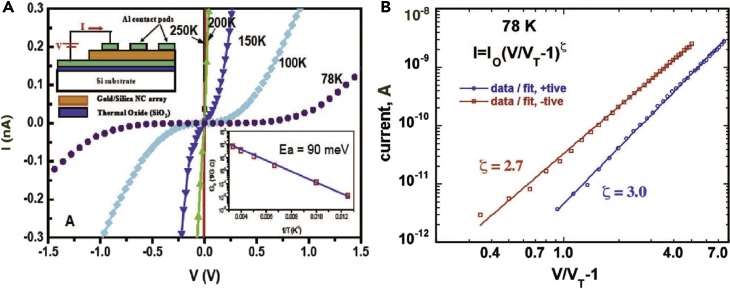
Figure 15.
Charge Transport in Thin Film of Gold NP/Silica Arrays
(A) I-V curves measured from 300 to 78 K. The inset shows a plot of the zero-bias conductance (G0) versus 1/T. The data exhibited Arrhenius behavior with activation energy (Ea) of ∼90 meV.
(B) At T = 78 K, the current displayed a power-law dependence for V>VT with scaling exponent ζ = 2.7 (negative bias) and ζ = 3.0 (positive bias).
Reproduced with permission from Fan et al. (Fan et al., 2004). Copyright 2004 AAAS.

