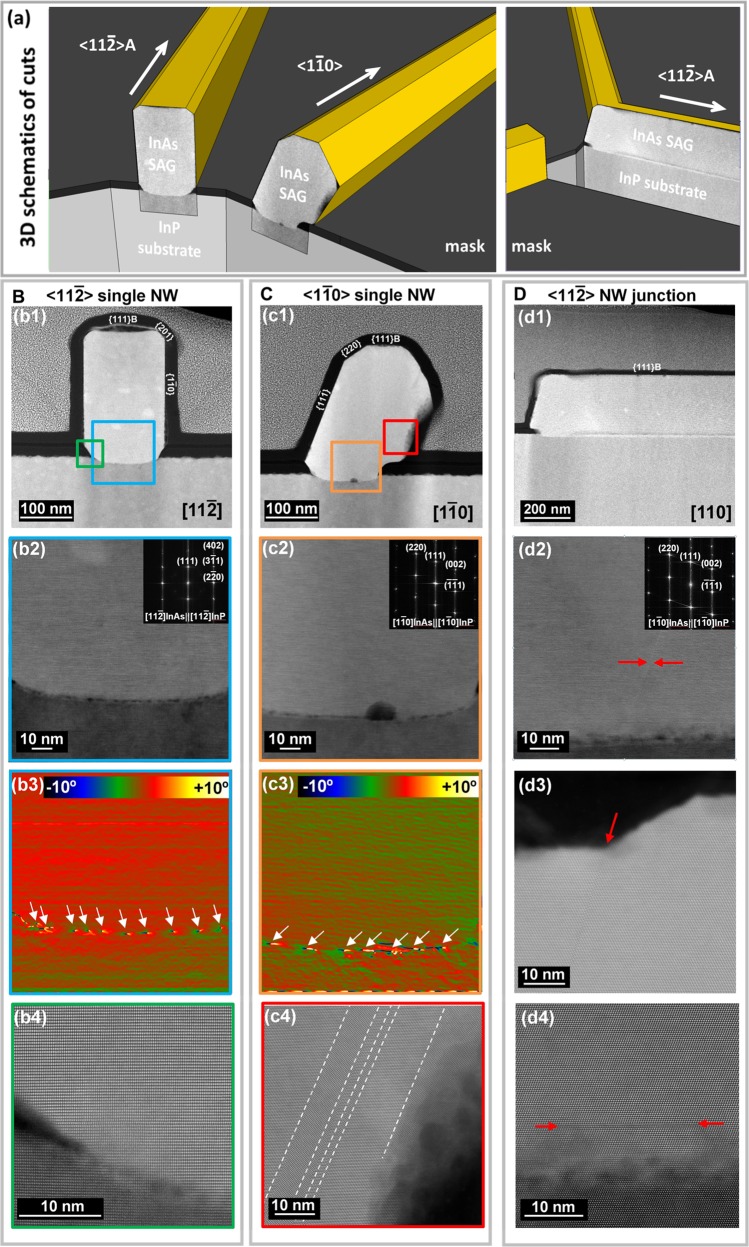
Figure 3.
Structural properties of in-plane InAs SAG NWs on InP(111)B substrates. (a) Schematics of the NW cross-sections under investigation: (left) perpendicular and (right) parallel to the NW in-plane direction. Panel B: cross-sectional STEM analysis of a < 112̅> nanowire observed through [12̅1] zone axis. (b1) Low-magnification HAADF-STEM micrograph showing an overview of the cross-section and faceting. (b2) Atomic-resolution HAADF-STEM micrograph with the corresponding fast Fourier transform (FFT) power spectrum. (b3) Rotational map obtained in the (22̅0) planes highlighting the presence of periodical misfit dislocations at the InAs–InP interface (white arrows). (b4) Details on the atomic arrangement near the interface with the substrate and mask. Panel C: cross-sectional STEM analysis of a < 11̅0>-oriented nanowire observed through [11̅0] zone axis. (c1) Low-magnification HAADF-STEM micrograph of cross-sectional cut. (c2) Atomic-resolution HAADF-STEM image with the corresponding FFT and plane identification on the sample interface. (c3) Rotational map applied to the (1̅1̅1̅) planes highlighting the presence of the misfit dislocations at the InAs/InP interface (white arrows) and (c4) HAADF-STEM image on the overgrown region at the right showing the presence of twin boundaries (white dashed lines). Panel D: Longitudinal cross-sectional HAADF STEM of a < 112̅> -oriented NW junction observed through [11̅0] zone axis. (d1) Low-magnification overview of the cut. (d2) Interface with a propagating stacking fault (red arrows). (d3) Stacking fault creating the step on top of the NW and (d4) in-plane stacking fault originating just above the InAs–InP interface.

