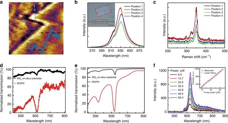
Fig. 2. Characterizations of the WOFN structure.
a Atomic force microscopy (AFM) image of a piece of WS2 on a sapphire substrate. The thickness of the WS2 film is ~0.6 nm, as shown in the inset. The scale-bar is 500 nm. b PL spectra of a transferred WS2 film on a glass slide and silica OFN; 1–4 denote the different positions labeled in the inset, at which the spectra are collected. The red dashed boxes outline the positions of the transferred WS2 on the WOFN and the residual WS2 film on the glass substrate. The scale-bar corresponds to 20 μm. c Raman spectra of the sample from the positions in b. d Measured normalized transmission spectra of the WOFN and WS2 on a silica substrate. The diameter of the OFN is ~800 nm, while the effective laminated length of WS2 on the WOFN is ~60 μm. e Calculated transmission spectra with the same structure parameters as those in d. f PL spectra of the WOFN with different pump power values (at 532 nm). The inset shows the linear relationship between the PL intensity and the pump light power

