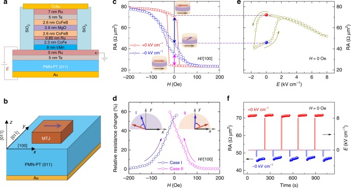
Fig. 1.
Non-volatile electrical manipulation of MTJs. a Schematic of the MTJ device structure deposited on PMN-PT. Voltage was exerted on the FE substrate to avoid damaging the MTJs. b Crystal orientation of the PMN-PT (011). The pinning direction of MTJ is along the [100] direction, represented by the purple arrow. x, y, and z edges denote the pseudocubic [100], [], and [011] crystallographic directions of PMN-PT, respectively. c MR curves measured at E = ±0 kV cm−1 after applying 8 kV cm−1 and −1.6 kV cm−1, respectively. The RA plotted here is the tunnel resistance for a circular shape with a 10 μm diameter. The insets illustrate the relative magnetization alignment around zero magnetic field. d Relative resistance change between E = ±0 kV cm−1 for case I and case II, illustrated by purple and red double-headed arrows in c respectively. The insets show schematic of magnetization configuration for case I and case II. The dark arrow denotes the magnetization of the pinned layer, which is fixed around H = 0 Oe. The red and blue arrows denote the magnetization of the free layer at E = ±0 kV cm−1, respectively. e Dependence of RA on electric field under H = 0 Oe for case I. The two distinctive resistive states at E = 0 kV cm−1 indicate non-volatile and reversible electrical manipulation of MR in MTJs. f Repeatable bistable resistance states modulated by 8 kV cm−1 and –1.6 kV cm−1 electric-field pulses in the absence of a bias magnetic field

