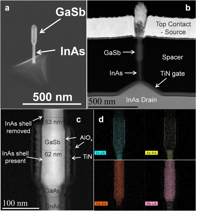
Figure 2.
(a) SEM image of an as-grown InAs stem, GaSb core, InAs shell nanowire. (b) and (c) HAADF STEM image of a fabricated VGAA NW GaSb-InAs C-S TFET with GaSb core diameter of 53 nm and InAs shell of 4.5 nm (d) EDX maps of Ga (orange), As (yellow), In (light blue), and Sb (purple). In (c) it is evident the InAs shell is etched in the region above the gate metal by the reduction of the NW diameter. In the EDX spectra, the brighter In and As signals at the edges of the NW also reveal the presence of a shell. The GaAs segment is also evident and is approximately 24 nm long.

