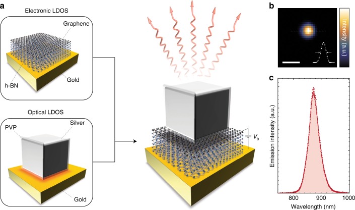
Fig. 1.
Visualization of the vdWQT device concept. a Illustration (not to scale) of a gold–few-layer h-BN–graphene vdWQT device, integrated with a (silver, PVP-coated) nanocube antenna. In this device configuration, the electronic LDOS is controlled by the hybrid vdW heterostructure whereas the optical LDOS is governed by the nanocube antenna. Applying a voltage Vb across the insulating few-layer h-BN crystal results in antenna-mediated photon emission (wavy arrows) due to quantum tunneling. b, c Measured spatial (b) and spectral (c) photon distribution from a nanocube antenna coupled to a vdWQT device, demonstrating a diffraction-limited spot and a narrow emission spectrum. The inset in b shows a line-cut, featuring a line-width (FWHM) of ~460 nm, close to the expected value of λ/(2NA) ~ 480 nm. Scale bar: 1 μm

