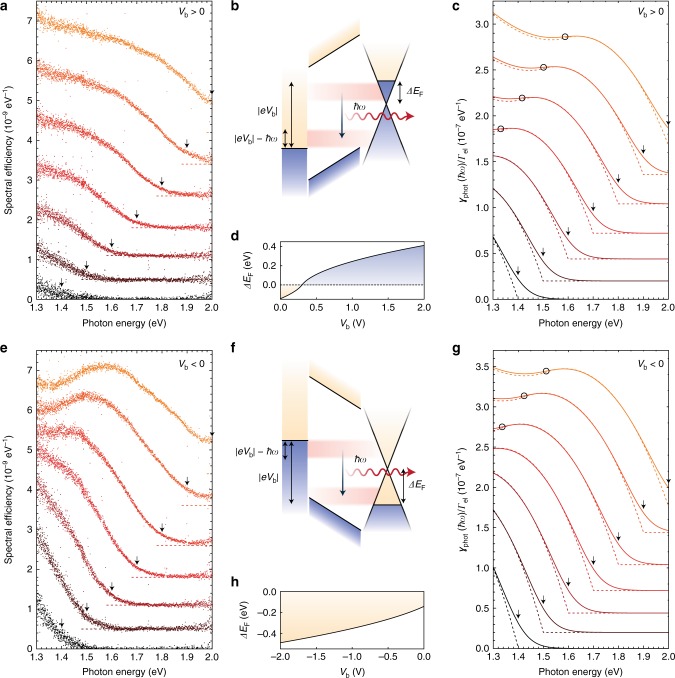
Fig. 4.
Spectral distribution of directly emitted photons from vdWQT devices. a, e Measured efficiency spectra (spectral distribution of emitted photons per tunneling electron, cf. Supplementary Note 1) for positive/negative voltages Vb from a Au–7L h-BN–Gr device. Subsequent spectra are acquired with increasing voltage from |Vb| = 1.4 V (black) to |Vb| = 2.0 V (orange) in steps of 0.1 V. Spectra are offset with respect to each other, dashed lines indicate the respective zero line. Arrows indicate the spectral position where ħω = eVb. b, f Schematic of inelastic electron tunneling at positive/negative voltages. Optical mode excitations (here: photons) are generated by spontaneous transitions from occupied states in one electrode to unoccupied states in the other electrode. The energy window available for spontaneous excitation of a mode of energy ħω is given by |eVb| − ħω. c, g Theoretical photon emission rate spectra (ρrad = 0.04ρ0) for positive/negative voltages Vb, normalized to the elastic tunneling rate Γel. Spectra are calculated for voltages from |Vb| = 1.4 V to |Vb| = 2.0 V in steps of 0.1 V. Straight and dashed lines show calculations for T = 300 K and T = 0 K, respectively. Black circles mark the positions on each curve for which the condition |eVb| − ħω = |ΔEF| is fulfilled. Arrows indicate the spectral position where ħω = eVb. d, h Electrostatically induced graphene Fermi level shift ΔEF (cf. Methods) as a function of (positive/negative) applied voltage

