Fig. 5.
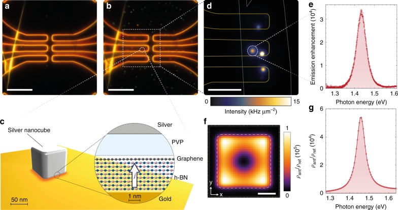
Nanocube antennas driven by a vdWQT device. a Darkfield microscope image of the same devices as shown in Fig. 2a. Scale bar: 10 μm. b Darkfield image after the deposition of silver nanocubes onto the sample. The red ring-like patterns on top of the electrodes indicate the presence of nanocube antennas. Scale bar: 10 μm. c Schematic illustration of the nanocube antenna configuration. The inset shows a vertical cross-section of the modified heterostucture configuration which determines the optical modes “seen” by tunneling electrons. d Spatial intensity distribution of light emission from nanocube antennas. Outlines indicate the spatial location of the edges of graphene and gold electrodes. Scale bar: 5 μm. e Emission spectrum of the antenna marked by a dashed circle in d at Vb = 2 V, normalized by the corresponding emission spectrum of the planar heterostructure (Fig. 4a). f Spatial (on resonance) and g spectral dependence of the simulated, radiative fraction of the optical mode density of the nanocube antenna ρant for a vertically oriented dipole located in the center of the h-BN crystal, normalized by the radiative LDOS of the planar geometry ρref, cf. Supplementary Note 4. The white dashed line in f marks the outline of the silver nanocube (75 nm with a 7.5 nm edge radius)

