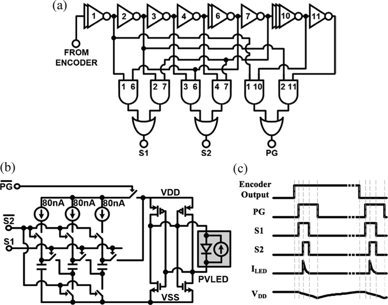
Fig. 6.
LED-driver circuits: (a) pulse generation circuitry: generates three pulses using a current-starved inverter chain and current-limited logic: a ~1 μs power-gating pulse (PG) to isolate the PVLED from VDD and the other two pulses (SI and S2) that reconfigure the charge pump from parallel to series to drive the LED; (b) charge pump and PVLED interface circuitry: during the normal, charging operation, MOS capacitors are connected to VSS and charged in parallel by 80 nA current sources, which are supplied from VDD that is connected to the positive node of the PVLED through the sign corrector circuit. During the LED pulsing mode, PG disconnects VDD to connect MOS capacitors, in series, to the LED; (c) timing diagram of the pre-described pulses, resulting current pulses, and VDD ripple.

