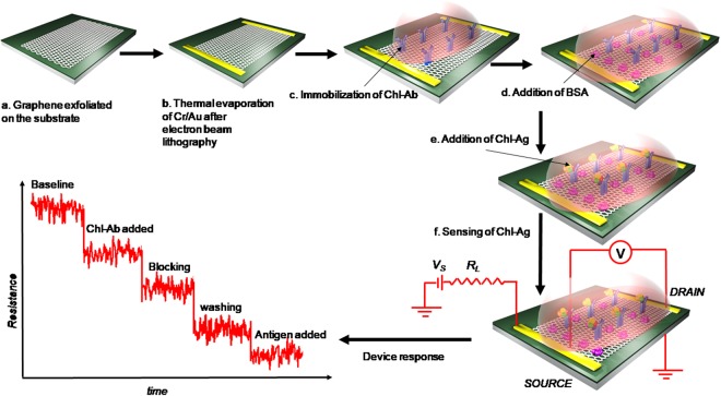
Figure 1.
Fabrication procedure for graphene FET device. (a) Graphene exfoliated on 285nmSiO2/Si substrate using scotch tape technique where SiO2 forms the back gate dielectric; (b) the graphene was electrically contacted by thermally evaporating 5/50 nm Cr/Au after electron beam lithography; (c) chl-Abs were immobilized onto graphene by carbodiimide activation that helps in the binding of the antibodies by covalent bonding; (d) Blocking was done with BSA in Phosphate Buffer, pH 7.4; (e) biosensing was performed by adding chl-Ag to the micro-device; (e) for measuring the response, a constant current circuit was used where Vs is the applied source voltage and RL is the current limiting resistance; and (f) the signal was measured by monitoring the resistance as a function of time for different concentrations of antigens.

