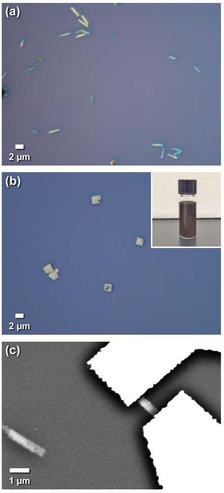
Figure 4.
Optical microscopy images of (a) SnS nanoribbons and (b) SnS square nanosheets dropcast from (inset) colloidal solution on p+Si/SiO2 substrates prior to device fabrication. (c) SEM image of a back-gated, 2-contact device fabricated from an individual SnS nanoribbon that was cast onto the substrate.

