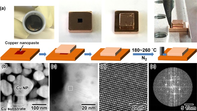
Figure 6.
Adhesion of the copper substrates with use of the copper nanopaste and the share strength of the die attach material. (a) Schematic and photo images for the preparation of a model IC chip-mounted die with use of the copper nanopaste and the die share stress measurement. (b) An HAADF-STEM image of the adhesion between copper NPs on the copper substrate. (c) A magnified image of the binding position between a copper NP and the copper substrate. The white-colored solid square shown in (b) is the magnified position. (d) An HAADF-STEM image to observe the crystallinity of the sintered position. The white-colored solid square exhibited in (c) is the magnified position. (e) A Fourier transfer image of (d). The bright spots could be assigned as (111) diffraction of Cu.

