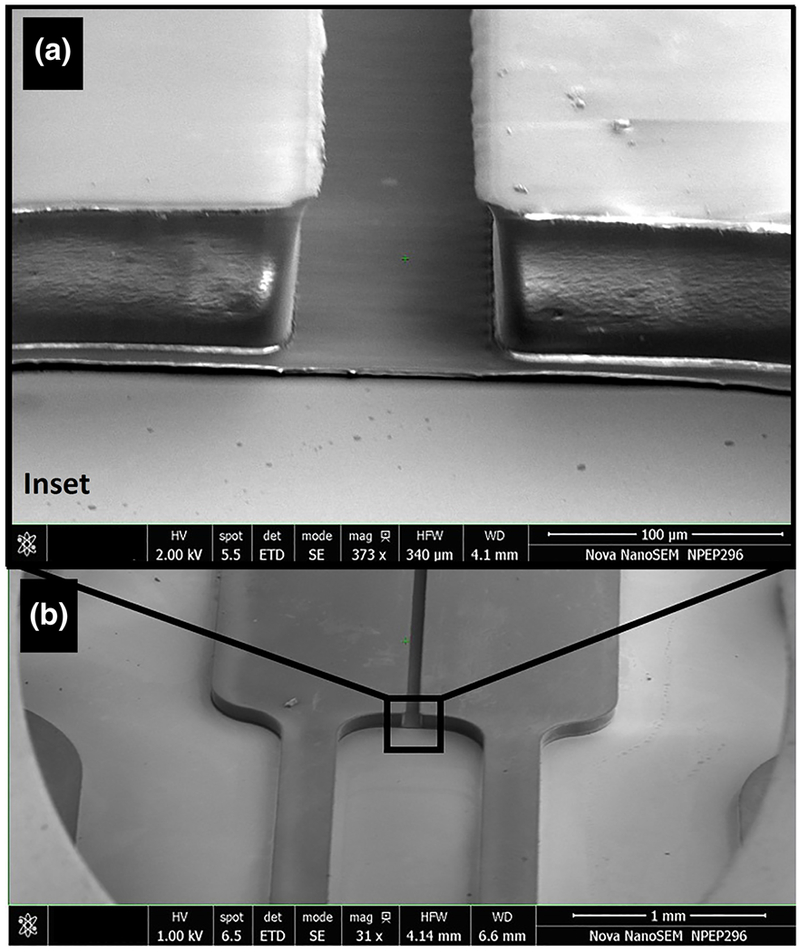
Fig. 3.

SEM of Mμn System. Profile view of patterned photoresist on the Si master mold after two-step photolithography process, demonstrating the tiered structure of the Mμn and fine channel detail. Cell seeding regions and the paired inlet/outlet ports are 50 μm in height and the channel array is 5 μm in height. Detail inset view (a) with macroscale view (b)
