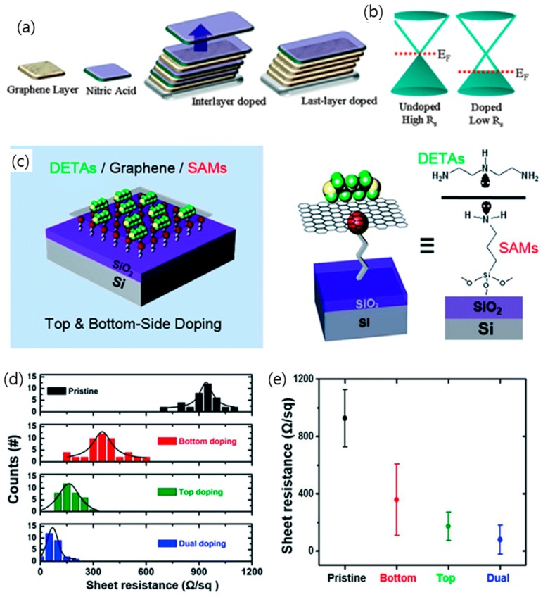
Figure 5.
(a) Schematic illustrating the interlayer doping methods. The sample is exposed to nitric acid after each layer is stacked. (b) Illustration of the graphene band structure, showing the change in the Fermi level due to chemical p-type doping. Reproduced with the permission of Reference [105]. Copyright 2010, American Chemical Society. (c) Dual-side doped graphene (left) and graphical representation of the molecular structure of the dopants on the both sides of graphene (right). (d) Histogram of the sheet resistance of graphene doped by NH2-SAMs, diethylenetriamine (DETA), and DETA/NH2-SAMs (dual-side doped). (e) Averages and distributions of the sheet resistance plot of four different types of graphene field-effect transistors (FETs). Reproduced with the permission of Reference [41]. Copyright 2014, Royal Society of Chemistry.

