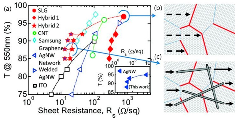
Figure 7.
(a) Optical transmittance at wavelength of 550 nm (T@550nm) vs. sheet resistance (RS) for previous experimental reports, including networks of carbon nanotubes, networks of silver nanowires (AgNW Network and Welded AgNWs), indium tin oxide (ITO), CVD-grown single-layer polycrystalline graphene (SLG) and graphene/NW hybrid structures with various nanowire densities. (b,c) illustrate the transport across grain boundaries (GBs) in CVD SLG and hybrid SLG AgNWs networks, respectively. Low-resistance grain boundaries (LGBs, blue lines) and high-resistance grain boundaries (HGBs, red lines) are shown. The HGBs dominate the resistance in SLG. In hybrid structures with appropriate densities of AgNWs, the NWs bridge the HGBs, providing a percolating transport path for the electrons and therefore lowering the sheet resist. Reproduced with the permission of Reference [51]. Copyright 2013, Wiley-VCH.

