Figure 2.
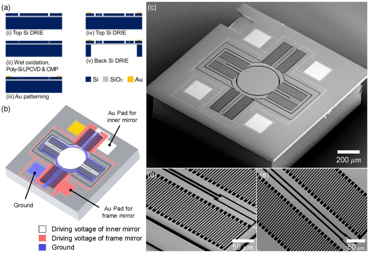
Microfabrication procedure and SEM images of HDHF Lissajous MEMS mirror. (a) Microfabrication procedure. The MEMS mirror was fabricated using a 6-inch SOI wafer with high conductivity. (b) A schematic of the electrical layout of the MEMS mirror. (c) Top SEM image of the microfabricated HDHF Lissajous MEMS mirror (scale bar: 200 μm). The physical dimensions of the MEMS mirror were 1.2 × 1.2 × 0.43 mm3. (d–e) Perspective SEM images of the comb drives of the inner mirror and the frame mirror, respectively (scale bar: 50 μm). The widths of the torsion bar were 2.8 μm and 8.8 μm in the inner mirror and the frame mirror, respectively.

