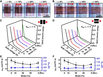
Fig. 3. Rubbery transistors under mechanical strain.

(A and B) Sequential optical microscopic images of the rubbery transistors under mechanical strains of 0, 10, 30, and 50% along (A) and perpendicular (B) to the channel length direction. (C and D) Transfer characteristics of the rubbery transistors under mechanical strains of 0, 10, 30, 50, and 0% (released) along (C) and perpendicular (D) to the channel length direction. (E and F) μFE and VTH of the rubbery transistors under mechanical strains of 0, 10, 30, 50, and 0% (released) along (E) and perpendicular (F) to the channel length direction.
