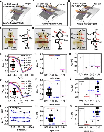
Fig. 4. Rubbery logic gates.

(A) Exploded schematic illustration of the rubbery inverter. (B) An optical image (left) and a circuit diagram (right) of the rubbery inverter. (C) VTC of the rubbery inverter under mechanical strains of 0, 10, 30, 50, and 0% (released) along the channel length direction. (D) VTC of the rubbery inverter under mechanical strains of 0, 10, 30, 50, and 0% (released) perpendicular to the channel length direction. (E) Voltage gain and VM of the rubbery inverter under mechanical strains of 0, 10, 30, 50, and 0% (released) along and perpendicular to the channel length direction. (F) Schematic exploded view of the rubbery NAND gate. (G) An optical image (left) and circuit diagram (right) of the rubbery NAND gate. (H) Schematic exploded view of the rubbery NOR gate. (I) An optical image (left) and circuit diagram (right) of the rubbery NOR gate. (J to L) Output characteristics of the rubbery NAND gate under VDD of 1 V under mechanical strains of 0% (J) and 50% along (K) and perpendicular (L) to the channel length direction. (M to O) Output characteristics of the rubbery NOR gate under VDD of 1 V under mechanical strains of 0% (M) and 50% along (N) and perpendicular (O) to the channel length direction.
