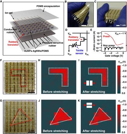
Fig. 5. Fully rubbery tactile sensing skin with an 8 by 8 active matrix.

(A) Schematic exploded view of the fully rubbery tactile sensing skin. (B and C) The optical images of the deformed fully rubbery tactile sensing skin under bending (B) and stretching (C). (D) The circuit diagram of one tactile sensing pixel. (E) Transfer characteristics of the rubbery transistor in the active matrix with and without applying pressure. (F and G) Optical image of the fully rubbery skin in contact with the custom made rubber block. (H and I) Output voltage mapping result before (H) and after (I) stretching along the channel length direction. (J and K) Output voltage mapping result before (J) and after (K) stretching perpendicular to the channel length direction.
