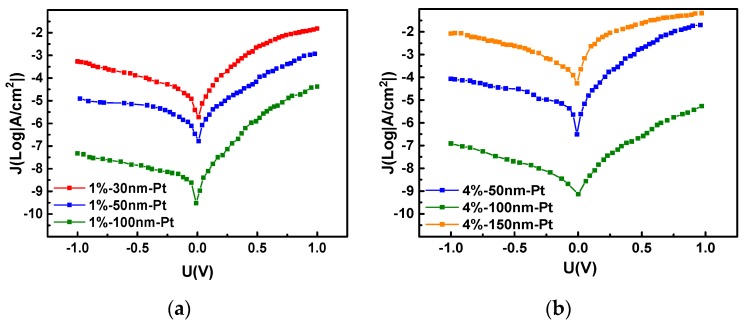
Figure 6.
J–V Characteristics of Pt/a-IGZO Diodes with Different a-IGZO Thicknesses. (a) J–V characteristics of Pt/a-IGZO diodes with a-IGZO thicknesses of 30, 50, and 100 nm, and sputtering process O2: (O2 + Ar) = 1%. (b) J–V characteristics of Pt/a-IGZO diodes with a-IGZO thicknesses of 50, 100, and 150 nm, sputtering process O2: (O2 + Ar) = 4%.

