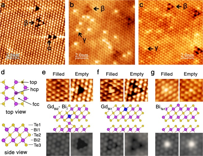
Figure 3.
Experimental and simulated STM images of x = 0.15 before and after annealing. (a) Empty-state scanning tunneling microscopy (STM) image for as-grown single crystal. The defects α and β are related with the Gd substitution. (b,c) Filled- and empty-state STM images after annealing. Notice that the α defects almost disappear, the β defects increase, and the γ defects are newly formed. (d) Schematic diagram of the atomic structure of pristine Bi2Te3: top view (upper) and side view (lower). The pink and yellow circles represent Bi and Te atoms, respectively. (e–g) Experimental high-resolution STM images (upper), atomic structures (middle), and simulated constant-current STM images (lower). (e) α defect: GdBi2-BiI, (f) β defect: GdBi1, and (g) γ defect: BiTe1. The simulated STM images are in good agreement with experiments. The blue circle represents Gd atom. The filled- and empty-state images are measured at VS = −0.35 and +0.30 V in as-grown sample and VS = −0.65 and +0.35 V in annealed sample, respectively, and simulated at VS = −0.6 and +0.6 V, respectively.

