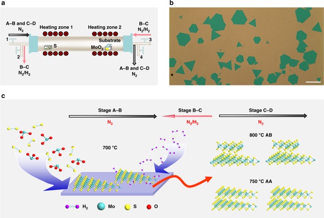
Fig. 1.
Reverse-flow chemical vapor epitaxy process for bilayer MoS2. a Experimental setup of the modified sequential two-stage thermal CVD process: A-B stage stands for the growth of first layer, C-D stage represents the growth of second layer, while B-C stage corresponds to the growth swing stage for the first and second layers. A reverse N2/H2 flow from the substrate to the source was introduced during the temperature swing stage (B-C stage). b A representative optical image of the as-grown bilayer MoS2 crystal grains. The scale bar is 100 μm. c Schematic diagram of the reverse-flow chemical vapor epitaxy process for bilayer MoS2. Different growing temperatures at C-D stage can result in bilayer MoS2 crystals with different stacking structures: 750 °C for AA stacking bilayer crystals and 800 °C for AB stacking ones

