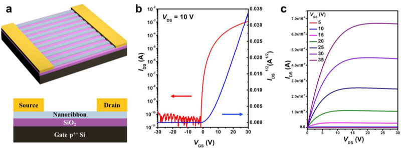
Figure 4.
(a) Schematic illustrations of an In2O3 field-effect transistor (FET) in a bottom-gate-top-contact configuration. Gate: Si (p++); Source/Drain: Au; semiconducting channel: In2O3 nanoribbons. The widths and lengths of the inter-digital electrodes are 1300 and 45 εm, respectively. The widths and pitches of the nanoribbons are 200 and 400 nm, respectively. (b) Transfer and (c) output characteristics of an ultrathin In2O3 nanoribbon FET, showing the measured current between the drain and source (IDS) in response to varying gate to source voltages (VGS) and source to drain (VDS) potentials, relative to the source. Devices displayed n-type pinch-off behavior with carrier motilities of 10.0 ± 2.6 cm2 V−1 s−1, averaged over 10 devices with a peak value of 13.7 cm2 V−1 s−1, and a current on/off ratio >107.

