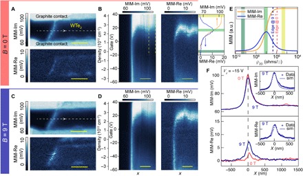
Fig. 2. Gate and magnetic field dependence of the edge conduction.

(A) MIM-Im and MIM-Re images of part of a monolayer WTe2 flake between two thin graphite contacts, measured at B = 0. (B) MIM-Im and MIM-Re obtained along the dashed line in (A) and stacked as a function of gate voltage. The corresponding carrier density is plotted on a separate axis, which includes an offset by the charge neutrality point. The upper right panel plots the averaged linecuts over the bulk region indicated by the two dashed lines in the MIM-Im channel, from Vg = −20 to 40 V. (C and D) Real-space images and gate voltage dependence at B = 9 T. (E) MIM-Im and MIM-Re signals as a function of 2D resistivity. The colored bands match those in the linecuts in (B), and the dashed lines indicate the 2D resistivity at the edge for B = 0 and 9 T, estimated from the line traces in (F). a.u., arbitrary units. (F) Averaged MIM-Im (top) and MIM-Re (bottom) traces of linecuts in between the two contacts with the edge position aligned at both B = 0 and 9 T. Insets are the comparison between the 9 T line traces and the simulated MIM responses. The measurement temperature is 5 K. Scale bars, 1 μm.
