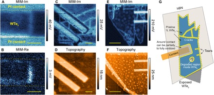
Fig. 4. Conductivity features near contacts and around defects in monolayer WTe2.

(A and B) MIM-Im and MIM-Re images of part of a monolayer (1L) WTe2 device between two Pt contacts, measured at T = 480 mK, Vg = 0 V, and B = 12 T. Scale bars, 500 nm. (C and D) MIM-Im and topography images of part of a second monolayer WTe2 device, measured at T = 10 K, Vg = 3.3 V, and B = 0 T. In the topography, the flake appears continuous, but MIM reveals that the regions around the contacts are highly insulating (dark). Scale bars, 1 μm. (E and F) MIM-Im and topography images of part of a third monolayer WTe2 device, measured at T = 10 K, Vg = 0 V, and B = 9 T. The small rings visible in the MIM-Im image correspond to the blisters in the topography image. Scale bars, 3 μm. (G) Cartoon illustrating various conductivity features observed in our experiments.
