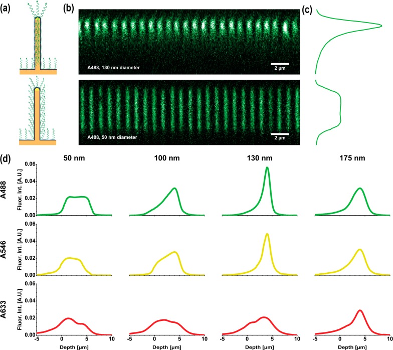
Figure 2.
(a) Schematic of the light emission pattern expected from lightguiding (top) and nonlightguiding (bottom) nanowires. (b) Confocal xz image (z-stack cross-section) of two A488-labeled nanowire arrays: 1 μm spacing, d = 130 nm (top) and d = 50 nm (bottom). The image of the thinner nanowires (bottom) shows homogeneous emission of light along the length of the nanowires, while the image of the thicker nanowires (top) shows emission increase at the nanowire tips, indicating that fluorescence emission couples into the nanowires and is guided to the tips. (c) Fluorescence intensity profiles obtained by averaging all nanowire profiles in the respective original images. (d) Representative fluorescence intensity profiles for nanowires of various d (left to right: 50, 100, 130, 175 nm) and with surface-attached fluorophores emitting at different wavelength ranges (see Supporting Information Section 3 for the emission spectra). Each profile shown is an average over several hundred nanowires. Profiles for all the tested d are available in Supporting Information Section 6. The profiles have been normalized to the area under the curve for visual comparison (details in Supporting Information Section 4).

