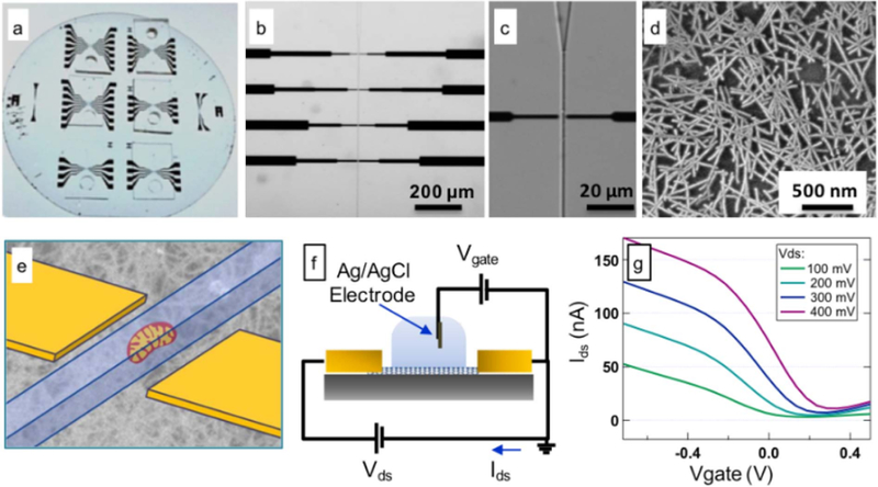
Fig. 1.

Structure and DC characterization of the mitochondrial nanoelectrode sensor device. (a) Optical image of the quartz wafer with 6 devices; (b) and (c) Bright field microscope images of the device with 20 × and 60 × magnifications; (d) Scanning electron micrograph exhibiting the carbon nanotubes deposited on the wafer surface; (e) Schematic showing the relative location of the carbon nanotube transistor and the flowing mitochondria; (f) Schematic showing the DC measurement set-up; (g) Drain-Source current Ids.vs. (electrolyte) gate voltage for a 3 µm × 3 µm device at different applied drain-source voltages.
