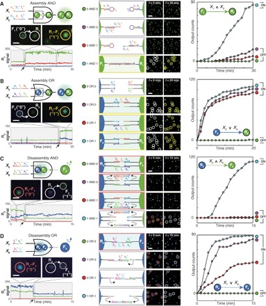
Fig. 2. Nanoparticle logic gates.

(A) Two-input Assembly AND. (B) Two-input Assembly OR. Assembly of G-NFs (F1) onto G-NRs (R1) and that of B-NFs (F2) onto G-NRs (R2) were traced as outputs for the AND and OR gates, respectively. (C) Two-input Disassembly AND. (D) Two-input Disassembly OR. Releases of G-NFs (F3) and B-NFs (F4) were traced as outputs for the Disassembly AND and OR gates, respectively. Each nanoparticle species is distinguished on the basis of its signal (color), mobility (R or F), and function (subscripted number). Domains a1t* and b1t [3 nucleotides (nt)] are truncated versions of a1* and b1 (6 nt), respectively. First column: Circuit diagram (top), actions of a single-nanoparticle logic gate in a logical TRUE condition (middle), and the time trace of a receptor signal (bottom). Solid and dashed arrows in the x axis indicate monomer-to-dimer and dimer-to-monomer transitions of receptors, respectively. Scale bars, 1 μm. Second column: Domain-level illustrations (left) and population-level responses (right) of the logic gates. Scale bars, 4 μm. Receptors are marked with white circles before assembly (red circles before disassembly) and yellow circles after assembly (gray circles after disassembly). Third column: Kinetics analysis. Each plot contains a reaction graph that corresponds to a logic gate. ∧ and ∨ denote the logic symbols for AND and OR, respectively. Legends are represented as truth tables. DNA sequences and experimental conditions are listed in tables S2 and S3. Experiments were carried out at 25°C in 1× phosphate-buffered saline (PBS) buffer.
