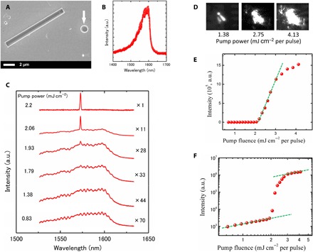
Fig. 2. Optical characterization at room temperature.

(A) SEM image of an InP/InAs MQD nanowire dispersed onto SiO2/Si substrates covered with a 200-nm-thick gold film for optical measurement. The white arrow indicates an indium particle moved from a nanowire tip in mechanical dispersion process. (B) PL spectrum of a single nanowire under a pump laser power of 0.83 mJ cm−2. (C) PL spectra of the nanowire with increasing pump power. The PL intensity continuously increases and eventually a narrow peak appears. Spectra are offset for clarity. (D) Far-field optical image of spatially resolved light emission from individual nanowires with increasing pump power. The diffraction fringes can be seen from the images with pump power of 4.13 mJ cm−2, indicating a lasing action. (E) L-L (light input-output) curve of the excitation power dependence. The curve reveals a transition from spontaneous emission to stimulated emission. The threshold power is estimated to be 2.15 mJ cm−2 per pulse. (F) L-L curve with semi logarithmic axis. Comparison of the measured output power data with a fit derived from the rate equations yields a spontaneous emission factor, β, of 0.0001 to 0.001. The S-shaped curve in the pump power dependence is indicative of the lasing action in the nanowire. a.u., arbitrary units.
