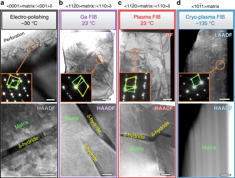
Fig. 1.
Transmission electron microscopy characterization. The bright-field TEM, SAED and STEM images for CP Ti prepared by a electro-polishing, b room temperature Ga-FIB, c room temperature Xe plasma FIB (Xe-PFIB) and d cryogenic Xe plasma FIB (cryo-PFIB). The scale bars represent 1 µm in the BF and 50 nm in the HAADF (a), 1 µm in the BF and 500 nm in the HAADF in (b, c), 500 nm in both the BF and the HAADF in (d). The inserts show the corresponding SAEDs indicating that the electron beam was close to the <0001> α, <112¯0> α, <112¯0> α and <101¯1> α zone axes for (a), (b), (c) and (d), respectively. Zone lines of each set of images are shown on top. The yellow and green lines in the insert SAEDs correspond to the diffraction reflections of δ-hydride and matrix, respectively. TEM transmission electron microscopy, SAED selected area electron diffraction, STEM scanning transmission electron microscopy, FIB focussed ion beam, HAADF high-angle annular dark field

