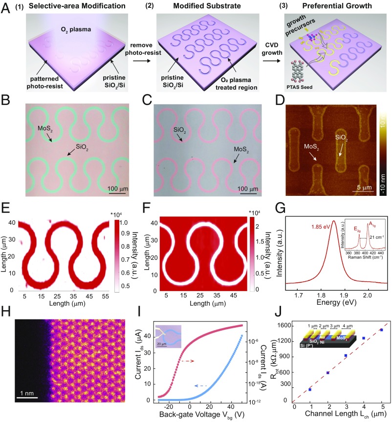
Fig. 1.
Patterned growth and characterization of MoS2 nanostructures. (A) Schematic representation of the procedures for the direct growth of MoS2 nanostructures via seed-promoted growth and substrate engineering. Step 1: the selective-area modification process by lithography patterning and O2 plasma etching; step 2: the patterned regions are distinguished from pristine SiO2/Si substrates after modification; step 3: the preferential growth of MoS2 on patterned SiO2/Si regions. (B) A typical OM image of a monolayer MoS2 wave array. (C) OM image of a monolayer MoS2 wave film that grows at the opposite locations when a negative photoresist was used for the wave pattern in B. (D) AFM image of a monolayer MoS2 kirigami structure showing the flat surface and ordered edge morphology. (E and F) PL mappings for monolayer MoS2 wave arrays and the inversed wave film pattern. (G) A typical PL spectrum collected on the monolayer MoS2 wave structures. (Inset) A typical Raman spectrum collected on the monolayer MoS2 wave structures. (H) ADF-STEM image of a patterned monolayer MoS2 edge showing the clean and ordered edge at atomic scale. (I) Transfer (Ids − Vbg) characteristic of a typical back-gated transistor fabricated on our CVD-patterned MoS2 film with gate voltages from −30 to 50 V and a bias Vds fixed at 1 V. The room temperature electron mobility of the transistor is 29.3 cm2 V−1 s−1. The red curve shows the transfer characteristic of the same MoS2 transistor in logarithmic scale. The on–off current ratio is ∼107. (Inset) Optical image of a typical MoS2 device based on the wave pattern. (J) Total device resistance RTOT normalized by width vs. channel length Lch measured at a carrier concentration n of ∼ 1.8 × 1012 cm−2, yielding a contact resistance of Rc ∼ 6.7 kΩ.µm from the vertical intercept. (Inset) The schematic of our TLM devices with Ni/Au contacts.

