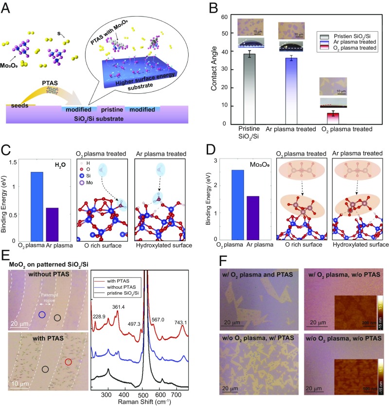
Fig. 2.
Mechanism study for the patterned growth of monolayer MoS2 nanostructures. (A) Schematic illustration of the growth mechanism of the patterned growth of MoS2. (B) Comparison of contact angles for pristine, Ar plasma-treated, and O2 plasma-treated SiO2/Si substrates. (C) DFT calculation for the binding energies between H2O and SiO2/Si substrate treated by O2 plasma and Ar plasma. (D) DFT calculation for the binding energies between Mo3O9 and SiO2/Si substrate treated by O2 plasma and Ar plasma. (E, Upper Left) OM image of MoO2 particles preferentially deposited on patterned SiO2/Si regions without PTAS. (E, Lower Left) OM image of MoO2 particles preferentially deposited on patterned SiO2/Si regions with the presence of PTAS. (E, Right) Raman spectra collected at the regions indicted by the red, blue, and black circles in the OM images in Left; several MoO2 Raman peaks are labeled in the spectra. It is shown that MoO2 particles exhibit a clear preference to deposit on the patterned region and that the Raman peaks of MoO2 are stronger with the presence of PTAS. (F, Upper Left) OM image of monolayer MoS2 flakes grown on O2 plasma-treated SiO2/Si substrate with the assistance of PTAS. The domain size of MoS2 is around 20 μm. (F, Upper Right) OM image of small MoS2 flakes grown on O2 plasma-treated SiO2/Si substrate without PTAS. (Inset) AFM images of MoS2 small flakes with domain size around 300 nm. (F, Lower Left) OM image of monolayer MoS2 flakes grown on pristine SiO2/Si substrate with the assistance of PTAS. The domain size of MoS2 is around 8–10 μm. (F, Lower Right) OM image of small MoS2 flakes grown on pristine SiO2/Si substrate without PTAS seed. (Inset) AFM images of MoS2 small flakes with domain size around 200 nm, indicating the poor quality of MoS2 growth.

