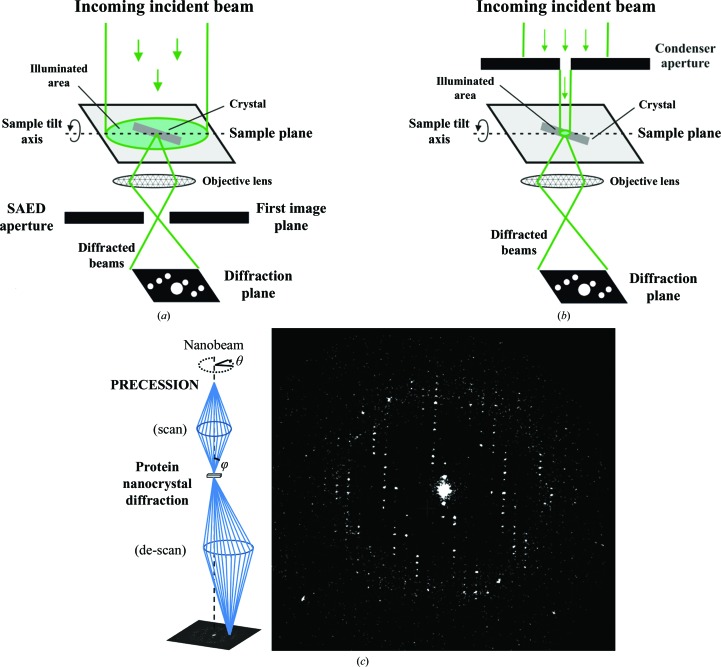
Figure 2.
(a) Sketch of the illumination conditions in the case of selected-area 3D electron diffraction. (b) Sketch of the illumination conditions in the case of nanobeam 3D electron diffraction. (c) Left: beam-path geometry in precession electron diffraction. Right: single pattern collected from a nanocrystal of HEWL in precession-assisted nanobeam 3D electron diffraction mode.

