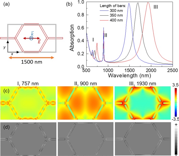
Figure 4.
(a) Scheme of a honeycomb lattice of bars. The grey line shows the simulation region, the black lines show the x- and y-axes and the polarization of the incoming wave has been depicted. (b) Absorption spectra for lattices of 1500 nm pitch, 45 nm width and 30 nm thickness and different lengths: 300 nm (blue), 350 nm (black) and 400 nm (red). (c) log(|E|2/|E0|2) and (d) charge distribution of the 400 nm bars lattice for the peaks labeled as I-III in (b) at z = 15 nm, being the origin (z = 0) located at the top of the dielectric layer.

