Fig. 6.
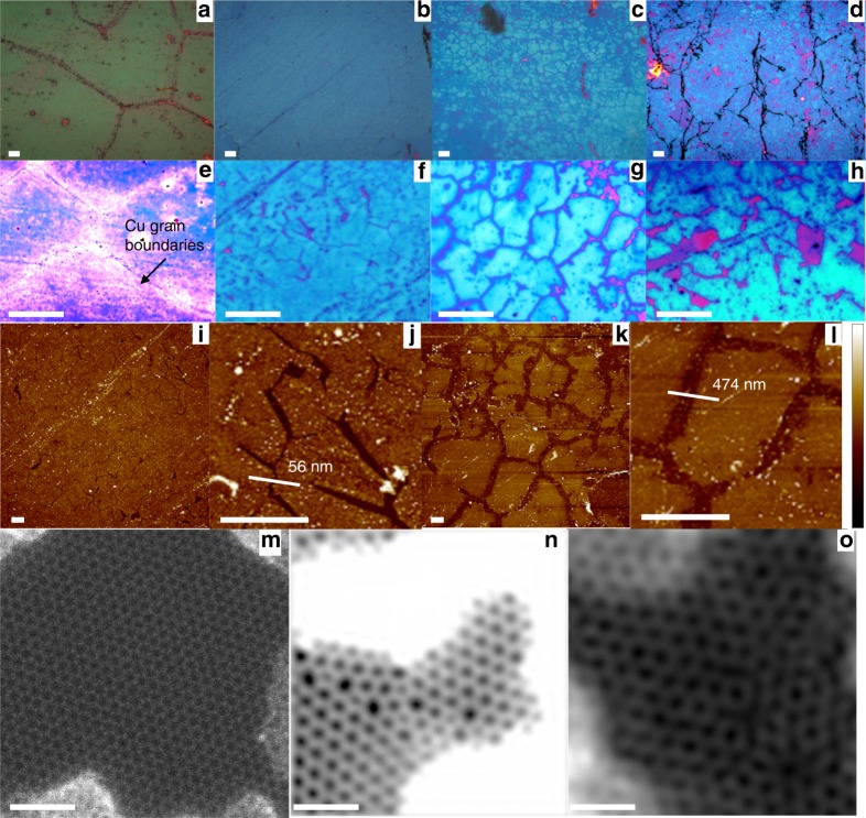
Visualizing defects. Optical images of Ge underlayer etched by water percolating through defects in the graphene overlayer. a–h Show results after the water percolation experiment on samples S1–4 as described in the text. a–d show the 5× images of the samples S1–4, whereas e–h show a higher magnification (50 ×) of the same sequence. Although a–d show large features such as Cu GBs, graphene GBs are clearly visible in f–h. In sample S1, visually coalesced graphene, the predominant defects lie at the GBs of the Cu foil when it is annealed for 2 h. Grains are 50–100 µm in size. In all other cases the defects lie at the coalescence boundaries, 5–10 µm apart, of the graphene monolayer. GBs in S2 annealed at higher supersaturation, are less defective than in S3, as indicated by the higher water percolation rates and hence more deeply etched boundaries. Even annealing in pure hydrogen, S4, only results in defects at the boundary and not within the grain. The purple patches in a–h correspond to graphene grains that have flaked off. The pink dots in h correspond to triple junctions. i 40 micron square AFM scan of surface of S2 after the percolation experiment. j 7 micron square AFM scan of surface of S2 after permeation experiment with line scan to show etch pit width. k 40 micron square AFM scan of surface of S3 after the percolation experiment. l 7 micron square AFM scan of surface of S3 after percolation experiment with line scan to show etch width. m Shows a pristine graphene lattice without defects in S1. n Shows a representative boundary in sample S1 with a tilt misorientation of 13.86°. o Representative boundary in sample S4 with a misorientation of 18°. Image contrast adjusted for better visibility. Scale bars: a–h 10 μm; i–l: 3 μm and m–o: 1 nm. Color bar for i–l: − 20 nm to 20 nm

