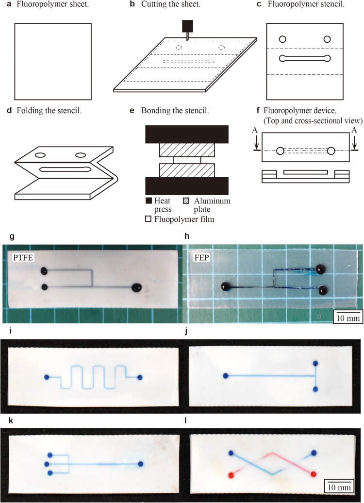
FIG. 1.
Fabrication of a fluoropolymer device using films. (a) and (b) A film of fluoropolymers (PTFE and FEP) was cut and patterned using a desktop cutting plotter. (c) A stencil of fluoropolymer was created. In this example, the stencil consisted of three (top, middle, and bottom) layers connected by dotted incisions. (d) The stencil was folded to create a device. (e) Heat and pressure were applied to seal the adjacent films in contact. (f) Schematic illustrations (top-down and cross-sectional) of the bonded films and [(g) and (h)] optical micrographs of the film devices entirely consisting of PTFE and FEP are shown. (i)–(l) Representative geometries of microchannels fabricated in PTFE. The channels are filled with water containing aqueous dyes.

